Let's try (3)
|
When ending drawing a schematic, the parts of the board are arranged out of the printed board. 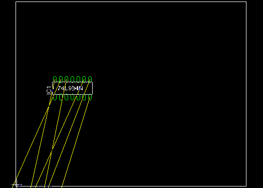 After pushing the Move button, it moves parts inside the white frame. 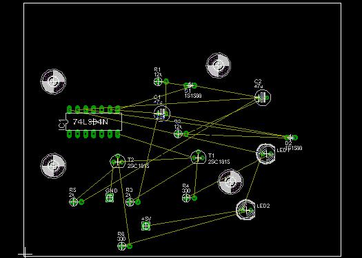 The yellow line shows a connection among the parts. The part should be arranged for the yellow line to become as short as possible. 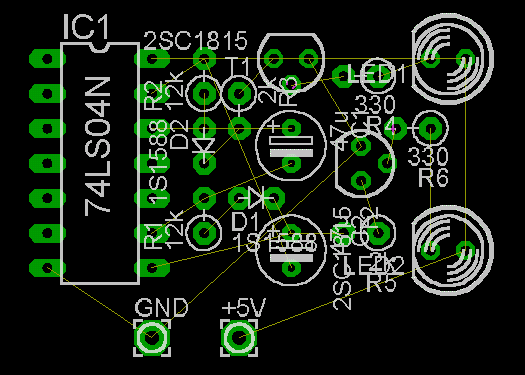 I did to the part arrangement which imitated the mounting of "A-stable multivibrator (IC type)".
 It selects "Display/hide layers..." from the pull-down menu of View menu in the board window. 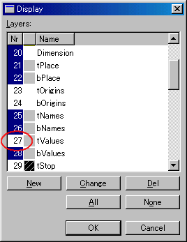 In this operation, the display dialog like the left is displayed. The item which is made blue in Nr is a displayed item. It clicks the part with the number of 27th(tValues) and changes into the white. In this operation, the display of the value which is put on the board can be suppressed. "t" at the head is the initial of TOP and it means the display of the component side of the board. "b" is the initial of BOTTOM and it means the display of the wiring side of the board. This time, there is no display item of the wiring side. So, the item of "b" is no effective. "Place" is the item which controls the display of the shape of the part. But, when making "Place" non-display mode, the name and the value of the same group(t or b) are suppressed both. Also, when making a display mode, all items of the group which is the same are displayed. "Origins" can do the operation of the name of the part. "Names" can control the display of the name of the part. "Values" can control the display of the value of the part. When suppressing the value of the parts, the display of the board is as follows.
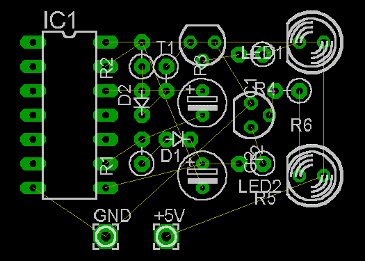  Let's wire automatically. Let's wire automatically.When pushing the Auto button, following dialog is displayed.
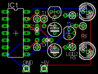
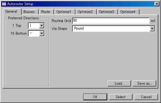 By setting the item of this dialog, the way of drawing a pattern can be controlled. This time, I drew a pattern without changing setting. When pushing the OK button, following pattern is drawn automatically. 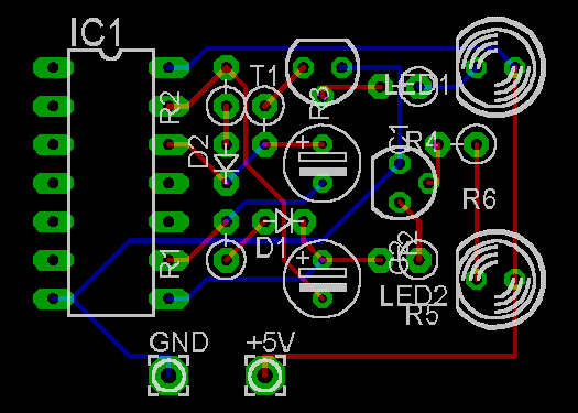 In EAGLE, a pattern is drawn using 2 layers (component side and wiring side) basically. The blue line is the wiring on the wiring side and the red line is wiring on the component side. When it isn't possible to draw a pattern normally, DRC(Design Rule Check) Errors is automatically displayed. The following error made display an error compulsorily to confirm an error display by the modification of the the distance data between PAD and wiring of the design rule after making draw a pattern normally. 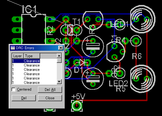
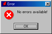
 When having closed DRC Errors window, it is possible to make display again with the "Errors" button. When having closed DRC Errors window, it is possible to make display again with the "Errors" button.When pushing the Errors button in the condition where a pattern is normally drawn, following message is displayed.
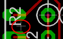
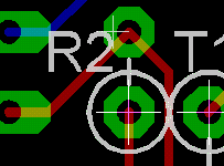
The display position of the name can be changed by the function of Smash, Rotate, Move. 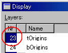 When controlling a name, Origins(23) of Display must be made effective. As for the way of displaying "Display dialog", refer to Display control of the part name and value. When making Origins effective, a centerline is drawn at each part.
As the example, I will describe using the name of R2.  First, pushe the Smash button.
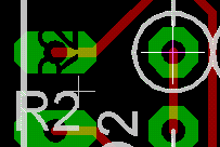
 Next, push the Rotate button and click the + mark which is put to the name.
 Next, push the Move button and click the + mark which is put to the name.
Lastly, adjust the hole to fix a printed board and the size of the printed board. 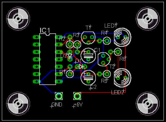
|
