Circuit explanation
of the frequency induction switch
 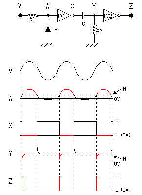 The pulse generation circuit changes the inputted analog signal into the pulse signal. It inputs the input signal to the inverter and it makes the rectangle wave. When the input terminal of the inverter is in the open condition, the input terminal becomes the high level (H) condition. Then, the inverter output is in the low level (L) condition. When the resistance value of R1 is small, the W point becomes below the threshold voltage (TH). This time, it becomes below TH because it used 1Kohm as R1. But, when the internal resistance of the signal generator which connects with the V point is high, it becomes above TH. When the W point is higher than TH, H and L of the signal of the X point reverse but don't influence the circuit operation. In any case, in the Z point, the pulse with the period which is the same as the input signal comes out. I do the following explanation, when signalless, it assumes that the W point is below TH. When the input signal is added in this condition, when becoming above the threshold voltage of the inverter, the output becomes the L condition. (The X point) The signal which was rectangular-ized in IV1 becomes the spike-shape signal with the differentiation circuit to compose in C and R2. (The Y point) The spike signal by the differentiation circuit does the waveform shaping with the inverter IV2. In the part below the threshold voltage of the signal which is added to the input of IV2, the output of IV2 becomes the H condition. In the interval of the output signal of IV2, it becomes the same as the period of the input analog signal. R1 and D are the one to protect IV1 when the excessive voltage is gained by the input. It uses the Zener diode for D, it passes the electric current to ground when the equal to or more than +5 V voltage is gained by the W point and the W point prevents becoming the equal to or more than +5 V voltage. As for the inverter, the input voltage, the input electric current characteristic depend on the kind (the bipolar, LS, HC). The circuit this time is using the LS type. As well as LS, it didn't work normally. If adjusting the output impedance(Resistance to the alternating electric current) of the signal generator, the value of R1, I think that it is possible to use the other type. Also, the characteristic of the input of the inverter has an influence on the characteristic of the differentiation circuit, too. Because it is, the pulse duration of the Z point can not be simply computed only at the value of C and R. Actually, attempted to change the value of C but the pulse duration doesn't change too much.  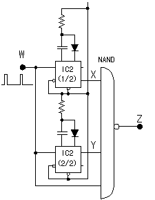 It is the circuit which checks whether or not the interval of the inputted pulse signal becomes the pulse interval of the rule. Because it is the same as the period of the input signal in the interval of the pulse, it checks whether or not the frequency of the input signal becomes the frequency of the rule. I used the IC which is called 74HC123 to check the interval of the pulse. This IC is called Retriggerable Single Shot. The two circuits are included in one piece of the IC. It has the function to reverse the condition of the output only in the constant time when the pulse is added to the input. The circuit this time uses two Single Shot circuits. I use the one for the frequency upper limit detection and other one for the lower limit detection. Retriggerable Single Shot 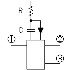 The reversing timing is when the input pulse changes into the L condition from the H condition. In the time (td) which the output reverses, it is decided by the value of R and C.
I don't understand the detailed data in case of 74HC123. This time, because R is more under 50K ohm, there is no problem.  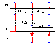 First, the case that the input frequency is within the detection frequency is explained. First, the case that the input frequency is within the detection frequency is explained.
The falling (H With this condition, the output Z point at the NAND1 gate becomes the L condition only among the tw. The Z point becomes the L condition in the interval of the input pulse only when entering between equal to or more than td1 + tw, equal to or less than td2. 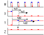 The upper limit timer is renewed in the falling of the input pulse. Because it is, when the interval of the input pulse is equal to or less than td1, after that, the X point doesn't become the H condition. The Z point is as the H condition. 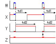 When the interval of the input pulse is more than td2(Strictly, it is above td2+tw), in the timing of the input pulse, the Y point becomes the L condition. The Z point is as the H condition.  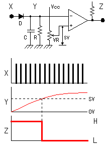 The input signal of the frequency induction switch circuit sometimes is not the single frequency. In case of the analog signal of the sound, the music and so on, in some moment, it becomes the detection frequency signal. The input signal of the frequency induction switch circuit sometimes is not the single frequency. In case of the analog signal of the sound, the music and so on, in some moment, it becomes the detection frequency signal.It is the duration detector that prevents the malfunction by it. The IC of the voltage comparator is used for the duration detection. It stores up the electric charge to C by the pulse signal which is added to the X point. When the electric charge stores up, the voltage of the both edges of C rises. It detects the rise of this voltage by the voltage comparator. It sets the reference voltage to compare to the the voltage comparator (+) input terminal. When the voltage of C which was connected with the (-) input terminal becomes above the reference voltage, the output of the comparator changes into the L condition from the H condition. When making the reference voltage high with VR, the detection voltage rises and when the voltage of C isn't high, the output doesn't change. Because it is, the output changes only when the pulse signal in the frequency detection range is continuously inputted. Discharging through R by the electric charge which was stored up in C with the pulse signal of the X point. Because it is, when the energy to discharge through R is bigger too much than the pulse energy of the X point, the voltage of C rises hardly. Discharging through R by the electric charge which was stored up in C and the voltage of C going down when the input pulse signal passes away. The diode D is to prevent discharging by the electric charge which was stored up in C when the X point becomes 0 V. When there is not D, the electric charge doesn't store up in C.  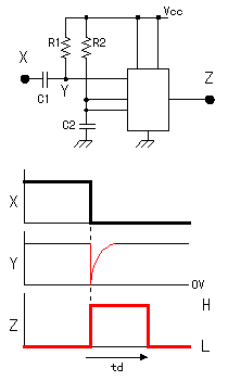 The output circuit outputs the H condition signal of the about 500 milliseconds when there is a continued detection frequency signal. I am using NE555 for the output circuit. When detecting the continued detection frequency signal, the X point changes into the L condition from the H condition. C1 and R1 compose the differentiation circuit. When the X point changes into the L condition from the H condition, the pulse signal which approaches 0 V occurs to the Y point. This signal becomes the trigger signal of NE555 and the output (the Z point) of NE555 becomes the H condition only in the constant time. In the time that the output of NE555 becomes the H condition, it is decided by the value of C2 and R2 and it is possible to calculate by the following formula.
At the circuit this time, I set to the about 500 milliseconds. |
||||||||||||||||||||||||||||||||