Making of the mask pattern
for the Double sided
|
I am using drawing software "Visio" to make the mask pattern of the printed board. Of course, you can use the other software, too. The first time in the use about me because this software had the symbol of the circuitry. As for Visio, refer to the following site. http://www.microsoft.com/office/visio/ As for the mask pattern making which used Visio, see "Making of the mask pattern by Visio". |
|||
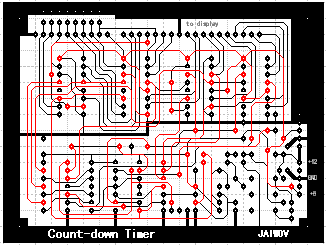
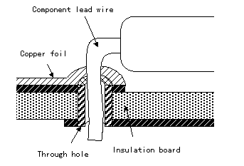
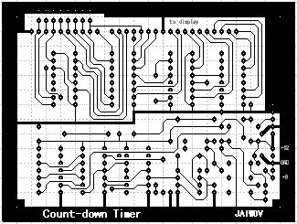
You can understand the point of the connection between the component side pattern and the wiring side pattern easily when making by one sheet of the drawing.  In the figure on the left, the black is the wiring side pattern and the red is the component side pattern. I made this pattern, presupposing the use of the through-hole. The red circle (the land) part shows the through-hole.  The through-hole is the way of connecting with the part which connects the component side pattern and the wiring side pattern through the thin metallic pipe. Because it is, the pattern of double sided can be connected in the place which solders the lead of the component. When not using the through-hole, you must solder the lead of the component at double sided. Or, it is necessary to connect using the wire in the place which is different from the lead of the component.
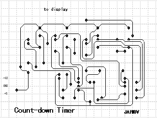
The pattern drawing for the component side and the wiring side is complete above. |

