Printing the mask pattern
[Menu]>[Manufacturing of Original PCB]>[The process of the PCB making]
|
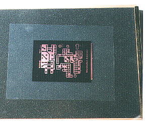
Make the sensitizer surface of the positive exposure printed board the upward and pile the film of the mask pattern on it. Adjust the position of the mask pattern carefully and fix it with the glass of the clamp equipment while careful so as not for the mask to shift. | 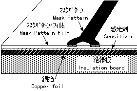 |
 |
|
|
Print the mask pattern using the fluorescence light. Set the clamp equipment which set the printed board, the mask under the fluorescence light. The ultraviolet rays in the sun are very strong and in the case in the daytime, the exposure completes as much as the 2 minutes. The ultraviolet rays of the fluorescence light are weak. About 20 minutes are necessary to expose. When the exposiong time is short, the long development time is necessary. | 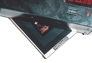 |
 It is exposing. |
|
|
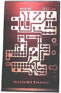
Put the board that the print of the mask pattern was ended in the developer of the sensitizer and it removes the unnecessary sensitizer. The part which the ultraviolet rays lashed dissolves in the developer and the copper foil appears. The part which the ultraviolet rays didn't lash doesn't dissolve in the developer and is left as the mask pattern. This mask pattern doesn't dissolve in the etchant. This time, in the development time, it was to be in the about 3 minutes. In the development time, it changes with the size of the printed board, the area which dissolves the sensitizer. Check the mask pattern carefully at this point. When the mask pattern is broken, repair in resist pen. When the pattern contacts next, shave with the cutter knife. Because the developer uses to remove the sensitizer of the mask pattern after the etching, you keep it. | 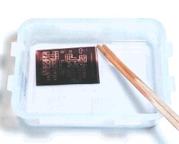 |
 |
|