Circuit explanation for A-stable multivibrator (TR type)
|
I will explain the operation of the circuit which is made this time.
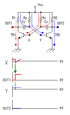
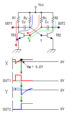
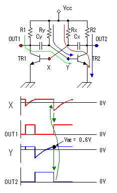
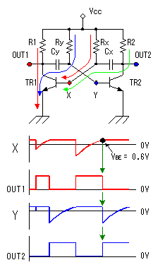
 When a power is supplied, the base electric current flows through TR1 through Rx, the base electric current flows through TR2 through Ry and TR1 and TR2 become the ON condition. Also, the electric current flows with R1  The collector electric current begins to flow when the base electric current flows as the operation of the transistor. The collector electric current can flow, that the hFE duple of the base electric current is done. However, the collector electric current of doing hFE duple doesn't flow. In case of TR1, the electric current of Vcc/R1 flows. For example, in case of Vcc = 5V, R1 = 1 K-ohm, hFE(the mu factor) = 100, IB(the base electric current) = 1 mA, in the calculation, it becomes the collector electric current of IB X hFE = 100 mA, but actually, only Vcc / R1 = 12 mA flow. In this case, even if it makes the base electric current more than 0.12 mA, the collector electric current doesn't increase. This condition is called the saturation state. Because it handles the 0 or 1 (ON or OFF) condition at the digital circuit, as the operation of the transistor, in case of ON, it uses in the saturation state. When applying the base electric current to the transistor, the voltage (VBE) between the base and the emitter becomes about 0.6 V. Even if the base electric current increases, this voltage doesn't change too much. After the X point is reduced to the negative voltage by Cx, the electric current flows through Rx in Cx. With this, the voltage of the X point rises gradually. When the X point becomes the 0.6 V, the electric current flows through Rx and TR1 changes into the ON condition rapidly. When TR1 becomes the ON condition, the Y point becomes negative with the electric charge of Cy.(This is called the reverse bias). This changes TR2 from the ON condition to the OFF condition. This condition lasts until VBE (the Y point) of TR2 becomes 0.6 V. Since Y points become minus voltage, the maximum permission voltage of VEB of a transistor is important. Since VEB is 5V in the case of 2SC1815, usage that the voltage applied to a capacitor exceeds 5V cannot be done. When supply voltage is set to 5V, LED of load is 2V and between the base and the emitter of a transistor is 0.6V, the voltage of a capacitor is 5 - 2 - 0.6 = 2.4V. Actually, it was a little less than 3V. The collector electric current begins to flow when the base electric current flows as the operation of the transistor. The collector electric current can flow, that the hFE duple of the base electric current is done. However, the collector electric current of doing hFE duple doesn't flow. In case of TR1, the electric current of Vcc/R1 flows. For example, in case of Vcc = 5V, R1 = 1 K-ohm, hFE(the mu factor) = 100, IB(the base electric current) = 1 mA, in the calculation, it becomes the collector electric current of IB X hFE = 100 mA, but actually, only Vcc / R1 = 12 mA flow. In this case, even if it makes the base electric current more than 0.12 mA, the collector electric current doesn't increase. This condition is called the saturation state. Because it handles the 0 or 1 (ON or OFF) condition at the digital circuit, as the operation of the transistor, in case of ON, it uses in the saturation state. When applying the base electric current to the transistor, the voltage (VBE) between the base and the emitter becomes about 0.6 V. Even if the base electric current increases, this voltage doesn't change too much. After the X point is reduced to the negative voltage by Cx, the electric current flows through Rx in Cx. With this, the voltage of the X point rises gradually. When the X point becomes the 0.6 V, the electric current flows through Rx and TR1 changes into the ON condition rapidly. When TR1 becomes the ON condition, the Y point becomes negative with the electric charge of Cy.(This is called the reverse bias). This changes TR2 from the ON condition to the OFF condition. This condition lasts until VBE (the Y point) of TR2 becomes 0.6 V. Since Y points become minus voltage, the maximum permission voltage of VEB of a transistor is important. Since VEB is 5V in the case of 2SC1815, usage that the voltage applied to a capacitor exceeds 5V cannot be done. When supply voltage is set to 5V, LED of load is 2V and between the base and the emitter of a transistor is 0.6V, the voltage of a capacitor is 5 - 2 - 0.6 = 2.4V. Actually, it was a little less than 3V.The electric charge begins to store up in Cx through R2 when TR2 becomes OFF. This becomes the preparation to do TR1 in the reverse bias to the next period. R2 and Cx compose the integration circuit. Therefore, even if TR2 becomes OFF, OUT2 doesn't stand up rapidly. When the value of R2 is big, the standing-up of OUT2 doesn't become the rectangle and becomes shaped like the integration curve. R1 in case of TR1 is same too. The electric charge stores up in Cy with the electric current which flows through Ry  The electric charge begins to store up in Cx through R2 when TR2 becomes OFF. This becomes the preparation to do TR1 in the reverse bias to the next period. R2 and Cx compose the integration circuit. Therefore, even if TR2 becomes OFF, OUT2 doesn't stand up rapidly. When the value of R2 is big, the standing-up of OUT2 doesn't become the rectangle and becomes shaped like the integration curve. R1 in case of TR1 is same too. The electric charge stores up in Cy with the electric current which flows through Ry TR2 changes into the ON condition when the Y point becomes 0.6 V. The X point is done in the reverse bias by the electric charge of Cx when TR2 becomes the ON condition and TR1 changes into the OFF condition. The electric charge is stored up through R1 in Cy and the preparation of the reverse bias of TR2 is done. The electric charge stores up in Cx through Rx This condition continues until the X point becomes 0.6 V.  TR1 changes into the ON condition when the X point becomes 0.6 V. The Y point is done in the reverse bias by the electric charge of Cy when TR1 becomes the ON condition and TR2 changes into the OFF condition. The electric charge is stored up through R2 in Cx and the preparation of the reverse bias of TR1 is done. The electric charge stores up in Cy through Ry This condition continues until the Y point becomes 0.6 V. It became the condition which was explained above in "Output's turning-over operation (1)". After that, it repeats this operation. |